Explore our premium select range of board-level array connectors, power storage units, and specialized capacitors.
Whitepaper Executive Summary on the Evolution of Micro-Pitch Interconnects and Power Systems
As electronic systems shrink in volume and expand in performance capabilities, the demand for sophisticated high-density array (HDA) connectors, custom backplanes, and low-impedance power storage systems has skyrocketed. High-density arrays serve as the nervous system in critical computing platforms, permitting high-speed signals to transition seamlessly between parallel PCBs with minimal insertion loss, reflection, or electromagnetic interference.
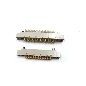
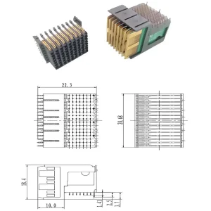
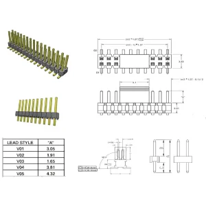
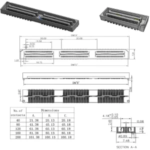
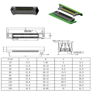
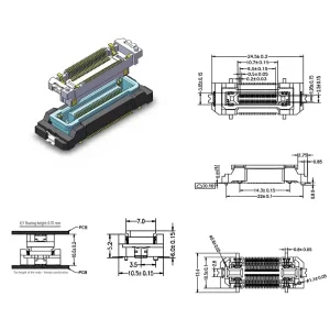
In modern industrial applications, achieving signal integrity up to 112 Gbps PAM4 requires microscopic precision during the design of pin-out grids and housing geometries. High-density mezzanine arrays operate under strict mechanical limits. A primary factor is coplanarity tolerance, which must be strictly maintained under 0.10mm across hundreds of contacts to ensure flawless surface mount technology (SMT) reflow processes. As an established OEM/ODM leader, Dynalink Electronic Technology Co., Ltd bridges this structural engineering gap through vertically integrated material synthesis, high-speed progressive die stamping, and rigorous environmental simulation.
Dynalink Electronic Technology Co., Ltd (DL), established in 2007, has evolved into a global powerhouse in the field of high-reliability components. Currently supporting a workforce of over 800 dedicated employees, among which more than 200 are specialized technical staff, Dynalink specializes in the high-end design, tooling, and precision manufacturing of custom power supplies, energy storage capacitors, and high-density electrical connectors.
Through our continuous capital commitment to research and development, we have built a fully integrated supply chain encompassing advanced metallurgy, polymer chemistry research, structure-based computer-aided engineering, and automated high-speed packaging. Our systems are certified under international management frameworks, guaranteeing compliance and reliability for long lifecycle operations.


Understanding Market Demands, Mechanical Constrains, and Signal Integrity Paradigms
The industrial market for interconnect technologies has entered an era governed by speed, spatial reduction, and extreme mechanical ruggability. System designers in sectors such as high-performance computing (HPC), aerospace computing systems, and automated automotive assemblies no longer view connectors as simple passive boundaries. Instead, high-density arrays are treated as complex transmission lines. Variations in pin geometry, contact materials, and mounting styles directly influence overall signal propagation speeds and system-wide thermal dissipation profiles.
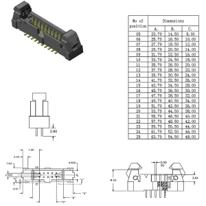
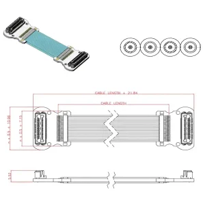
From a global commercial perspective, there is a clear trend toward multi-board modular designs like mezzanine setups and VPX architecture systems. These environments rely on hundreds of signal pins spaced at pitch dimensions of 1.27mm, 0.80mm, or 0.50mm. Maintaining consistent impedance characteristics (e.g., 85Ω for PCIe systems or 100Ω for Ethernet architectures) requires selecting polymer insulators with extremely low dielectric constants. Liquid Crystal Polymer (LCP) has become the industry standard for connector housings due to its excellent dimensional stability at elevated temperatures, allowing connectors to survive typical lead-free SMT assembly lines without warping or degradation.
| Interconnect Type | Common Pitch Settings | Target Impedance | Ideal Application Domain |
|---|---|---|---|
| VPX Slot Backplanes | 1.27mm to 2.54mm | 85Ω to 100Ω | Defense Avionics, Military Compute Systems |
| High-Speed Mezzanine Arrays | 0.50mm to 1.27mm | 85Ω to 90Ω | Data Centers, AI Accelerators, Telecom |
| Floating Board-to-Board | 0.50mm to 2.00mm | 90Ω to 100Ω | Automotive ADAS, Robotics, Smart Factory |
| Rectangular CRM Connectors | Custom Grid Layouts | Custom Matched | Medical Scanners, Railways, Avionics |
Unmatched expertise, vertically integrated engineering, and end-to-end design adaptability.
Our micro-array connections and power delivery profiles ensure stable high-amperage battery charging/discharging and continuous signal control under intense vibration environments.
We deliver ultra-low loss backplane systems and stable power supplies designed to handle massive transmission requirements, minimizing signal latency and thermal build-up.
Providing high-protection connector solutions (IP67/IP68 rated) that thrive in corrosive environments, high temperature spikes, and environments with heavy EMI.
Leveraging our internal intelligent design and simulation software, we can quickly build customized pin configurations, housing sizes, and tailored contact materials.
We push performance limits, designing tomorrow's solid-state battery interfaces, higher density capacitor modules, and board-level array terminals.
How Modern Engineering Solutions Resolve Real-World Connectivity and Power Issues
High-density arrays function as critical connection points in modern high-reliability equipment. Understanding their use in local, real-world deployment scenarios reveals how specialized material selections, mechanical layouts, and electrical properties work together to prevent system failure.

We prioritize strict quality standards, refining our processes to manufacture high-performance components that serve as industry benchmarks.
We aim to empower lives with technology and build a sustainable future. Our goal is to be a top-tier provider of integrated power, capacitor, and connector systems by working with integrity and innovation.
We encourage a collaborative, positive workplace. Supporting our employees' growth is central to our success, and we offer clear career paths alongside structured technical training programs.
We focus on continuous improvement across our product lines, working to refine solid-state battery designs, increase capacitor energy storage density, and build high-precision, low-loss connectors.
A Multi-Year Vision for Miniaturization, Thermal Management, and Ultra-High Frequency Operation
Dynalink's engineering division continues to refine our product capabilities. Our long-term roadmap focuses on addressing the physical limits of materials and manufacturing. This includes reducing pitch sizes, improving thermal performance, and maintaining signal integrity at higher frequencies.
As pin spacing decreases below 0.50mm, standard glass-reinforced polymers can fail during SMT reflow. To address this, we use advanced Liquid Crystal Polymers (LCPs) filled with mineral fibers. This compound features a low coefficient of thermal expansion (CTE) that matches copper and FR4 boards, preventing the connector from bending or flexing during high-temperature assembly.
For contact design, we utilize finite element analysis (FEA) to model insertion forces and contact pressure. We balance these mechanical properties with electrical performance by using specialized copper alloys like C18080, which offers excellent conductivity and resistance to thermal stress. Selective gold plating in the contact area ensures low resistance, while matte tin plating on the solder tails guarantees clean solder connections.
Our signal integrity laboratory is equipped with high-frequency network analyzers and simulation tools. This equipment allows us to analyze how changes in pin geometry impact insertion loss, return loss, and crosstalk. By optimizing the transition zone where the pin meets the PCB pad, we can design array connectors that support clean data transmission at speeds up to 112 Gbps PAM4, matching the requirements of PCIe Gen 6 and high-speed Ethernet standards.
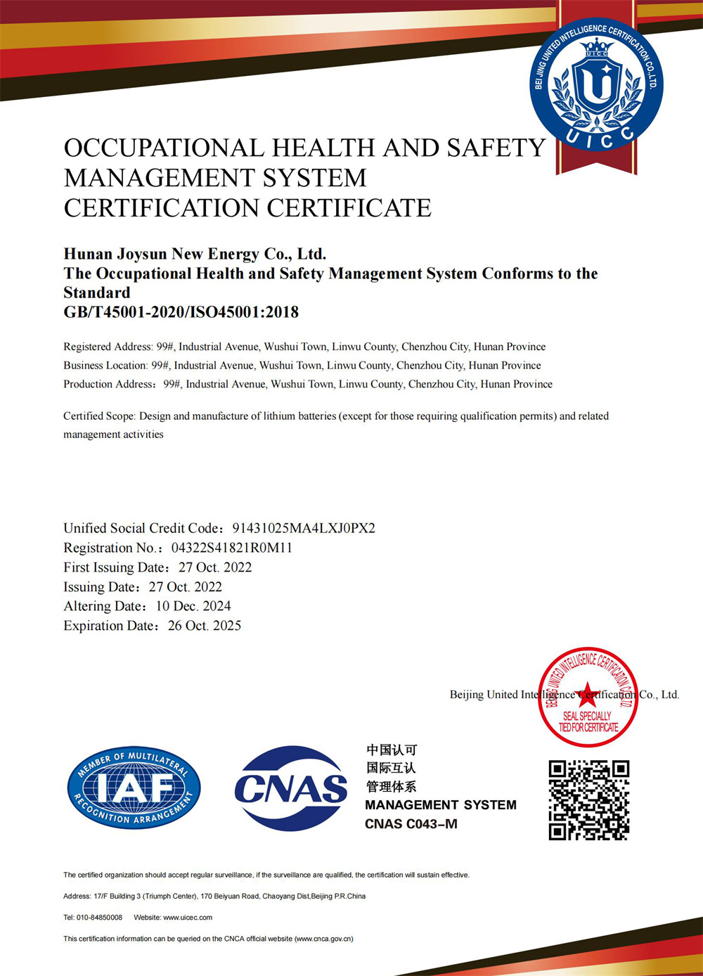
Meeting Global Quality, Environmental, and Safety Standards


Dynalink's Direct Vertical Integration Capabilities from Tooling Design to Final Production
Working with Dynalink as your manufacturing partner offers significant supply chain advantages. Our operations are base-structured in China's industrial zones, giving us direct access to raw materials, rapid tooling services, and experienced technical talent. By managing all manufacturing stages in-house—including design, precision tooling, metal stamping, plastic molding, plating, and testing—we maintain tight control over product quality and delivery schedules.
Managing the plating process internally is a key capability. Connector performance relies heavily on the quality of the gold plating layers. Dynalink uses automated plating lines that can apply selective gold coating with high precision. This allows us to place gold only on the functional contact areas, minimizing the use of precious metals to keep costs competitive while meeting performance specifications.
Additionally, our factory utilizes automated optical inspection (AOI) systems on the assembly lines. These systems inspect every connector for pin alignment, coplanarity, and housing defects. This level of quality control ensures that our products perform reliably in high-volume assembly processes and harsh field conditions.
Direct Engineering Answers Regarding Design Parameters, Material Choices, and Quality Control
Complete your system integration with our high-power jump starters, micro-pitch headers, and robust floating array series.